


2. Limitations of the Study
This study is based on a bibliographic patent portfolio and public patent/NPL records. The uploaded portfolio does not contain full claim text, abstracts, or complete descriptions for each family; therefore, patent-specific technical relevance should be confirmed through individual claim and specification review before relying on any family for legal or invalidity analysis.
3. Technical Background: From CRT Displays to MicroLED Displays
Display technology has evolved from bulky cathode-ray tube (CRT) systems to flat-panel and self-emissive display architectures. CRT displays generated images by scanning electron beams across phosphor-coated glass screens, but their size, weight, power consumption, and limited form-factor scalability led to the adoption of flat-panel technologies such as LCD and plasma displays.
LCD technology improved display thickness, power efficiency, and manufacturability by using liquid-crystal shutters with backlighting, while OLED introduced self-emissive pixels capable of high contrast, wide viewing angles, and flexible form factors. However, LCDs remain dependent on backlight and color-filter structures, and OLEDs face limitations related to material degradation, burn-in, peak brightness, and lifetime under high-luminance operation.
MicroLED displays advance this evolution by using microscopic inorganic LED chips as individual self-emissive pixels or sub-pixels. Compared with LCD and OLED, MicroLED offers high brightness, fast response time, high contrast, long lifetime, and improved stability. The main technical challenge is not the light-emitting principle itself, but the scalable integration of millions of MicroLEDs through mass transfer, bonding, inspection, repair, color conversion, and active-matrix backplane control.
3.1 MicroLED Process Flow
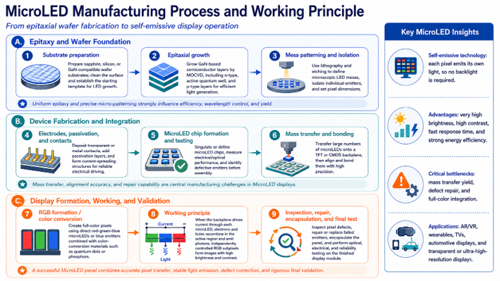
Figure 5: MicroLED Process Flow
The figure presents the MicroLED manufacturing process and working principle as an end-to-end device-fabrication and display-integration workflow that begins with substrate preparation, epitaxial growth, and mesa patterning on sapphire, silicon, or GaN-compatible wafers. The wafer foundation stage establishes the semiconductor layer stack, including n-type layers, active quantum wells, and p-type layers, followed by lithography and etching to define isolated microscopic LED mesas for individual pixel emitters.
The patterned MicroLED structures are then processed through electrode deposition, passivation, contact formation, chip definition, and electrical/optical testing. Defective emitters are identified before assembly, while functional MicroLED chips are transferred in large numbers onto a TFT or CMOS backplane through high-precision mass-transfer and bonding processes. This integration stage is critical because transfer accuracy, bonding reliability, and defect-repair capability directly affect display yield and manufacturing scalability.
The display-formation stage creates full-color pixels using direct RGB MicroLEDs or blue MicroLED emitters combined with color-conversion materials such as quantum dots or phosphors. During operation, the backplane selectively drives current through each MicroLED, causing electron-hole recombination in the active region and resulting in photon emission. Independently controlled RGB subpixels generate the final image with high brightness, high contrast, fast response time, and strong energy efficiency.
The completed panel is subjected to inspection, defect repair, encapsulation, and final optical, electrical, and reliability testing. Overall, the figure highlights MicroLEDs as self-emissive display devices that do not require a backlight, while also identifying key manufacturing bottlenecks such as mass-transfer yield, pixel-level defect repair, and full-color integration.
4. Technical Evolution and Research Direction
MicroLED has evolved from basic miniaturized inorganic LED display structures into a scalable display-manufacturing architecture that combines wafer-level epitaxy, micro-scale chip fabrication, mass transfer, full-color pixel formation, electrical bonding, defect detection, thermal control, and backplane integration. The major technical shift is from simply forming microscopic LED emitters to building a high-yield manufacturing flow that can place, connect, inspect, repair, and operate millions of MicroLED pixels with high accuracy and long-term reliability.
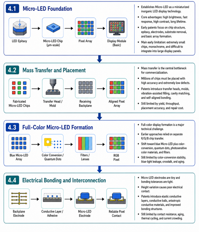
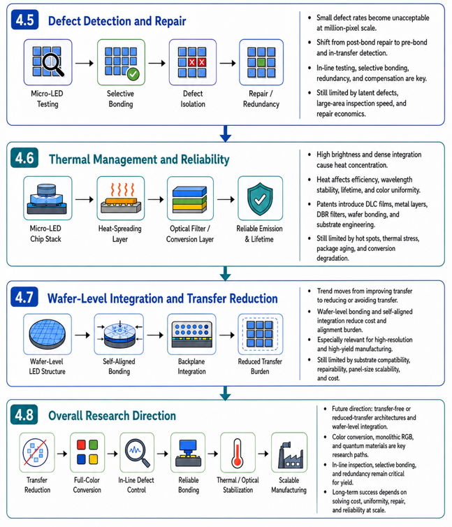
In summary, modern MicroLED technology is no longer limited to basic LED chip formation or simple pixel-array construction. It is becoming a complete display-integration platform where epitaxy quality, transfer accuracy, bonding reliability, full-color conversion, defect repair, thermal stability, and scalable manufacturing operate together. The best research directions are those that reduce or avoid mass transfer, improve wafer-level integration, enable stable full-color emission, support in-line defect control, and deliver reliable large-area display production at commercially acceptable cost.
4.1 MicroLED Foundation
This stage establishes MicroLED as a miniaturized inorganic LED display technology. The process begins with LED epitaxy, where semiconductor layers are grown on a substrate to form the light-emitting structure. These layers are then processed into micro-scale LED chips, arranged into a pixel array, and integrated into a basic display module. Early development mainly focused on chip structure, epitaxial quality, electrodes, substrate removal, and basic array formation. The main limitation at this stage is that the chips are extremely small, making them difficult to manufacture uniformly and integrate into large display panels.
4.1.1 Technical Terminology
- LED epitaxy: Growth of semiconductor layers used to form the LED light-emitting structure.
- MicroLED chip: A very small LED emitter, typically on a micrometer scale.
- Pixel array: Ordered arrangement of MicroLEDs forming display pixels.
- Substrate removal: Removing or separating the growth substrate after LED formation.
4.2 Mass Transfer and Placement
Mass transfer is one of the most critical bottlenecks in MicroLED commercialization. Since a display may require millions of MicroLED chips, each chip must be transferred from the fabricated wafer to the receiving backplane with very high positional accuracy and very low defect rate. Research and patents focus on transfer heads, molds, cavity matching, vibration-assisted filling, and self-aligned bonding to improve placement speed and yield. The key challenge remains maintaining throughput, alignment accuracy, repairability, and low cost at mass production scale.
4.2.1 Technical Terminology
- Mass transfer: Bulk transfer of many MicroLED chips from a donor wafer to a target backplane.
- Receiving backplane: Substrate containing drive circuitry where MicroLEDs are placed.
- Aligned pixel array: Properly positioned MicroLEDs forming accurate RGB or pixel structures.
- Yield: Percentage of successfully transferred and functional MicroLEDs.
4.3 Full-Color MicroLED Formation
Full-color MicroLED formation addresses how red, green, and blue pixels are generated. Earlier approaches used separate red, green, and blue MicroLED chips, but this increases transfer complexity. Newer approaches use a blue MicroLED array combined with color-conversion materials such as quantum dots or phosphors, along with filters or lenses, to generate RGB pixels. This reduces transfer burden but introduces challenges such as color-conversion stability, blue-light leakage, crosstalk, and aging.
4.3.1 Technical Terminology
- Quantum dots: Nanomaterials that emit specific colors when excited by light.
- Blue-light leakage: Unwanted blue light passing through color-conversion regions.
- Crosstalk: Optical interference between adjacent pixels or subpixels.
4.4 Electrical Bonding and Interconnection
This stage focuses on forming reliable electrical connections between MicroLED chips and the backplane electrodes. Because MicroLED electrodes are extremely small, bonding tolerances are tight, and even minor height variation can cause poor electrical contact. Patents introduce conductive adhesives, elastic conductive layers, conductive balls, anisotropic conductive materials, and improved bonding structures to ensure stable current delivery to each pixel. The remaining issues include contact resistance, aging, thermal cycling, and current crowding.
4.4.1 Technical Terminology
- Backplane electrode: Conductive pad on the backplane used to connect and drive the MicroLED.
- Contact resistance: Electrical resistance at the interface between two connected conductors.
- Current crowding: Non-uniform current flow concentrated in small regions.
4.5 Defect Detection and Repair
At a million-pixel scale, even a small defect rate can create unacceptable display quality issues. This stage focuses on identifying defective MicroLEDs through testing, isolating faulty pixels, and repairing or compensating them using redundancy or selective bonding. The technology is shifting from post-bond repair to pre-bond and in-transfer detection so that defective chips can be avoided before final assembly. The key limitations remain latent defects, inspection speed, repair economics, and large-area testing accuracy.
4.5.1 Technical Terminology
- Defect detection: Testing process used to identify non-functional or weak MicroLEDs.
- Repair/redundancy: Replacing, bypassing, or compensating defective pixels using spare structures.
- Latent defect: A hidden defect that appears after operation, stress, or aging.
4.6 Thermal Management and Reliability
MicroLEDs provide high brightness, but dense integration causes heat concentration. Excess heat can reduce efficiency, shift emission wavelength, degrade color uniformity, and shorten device lifetime. Research, therefore, focuses on heat-spreading layers, optical filters, conversion-layer stability, wafer bonding, substrate engineering, and protective materials such as DLC films or metal layers. The main challenges remain hot spots, thermal stress, package aging, and degradation of color-conversion materials.
4.6.1 Technical Terminology
- Optical filter: A layer used to control emitted light wavelength or block unwanted light.
- Thermal stress: Mechanical stress caused by temperature changes.
4.7 Wafer-Level Integration and Transfer Reduction
This stage represents a shift from improving mass transfer to reducing or avoiding it. Wafer-level integration and self-aligned bonding aim to integrate MicroLEDs directly at the wafer or panel scale, reducing the need for individual chip transfer. This approach can lower cost, improve alignment, and increase manufacturing yield, especially for high-resolution displays. However, it is still limited by substrate compatibility, repairability, panel-size scalability, and process cost.
4.7.1 Technical Terminology
- Wafer-level integration: Integration of MicroLED structures before singulation into individual chips.
- Self-aligned bonding: A bonding process where structures automatically align through geometry or material interaction.
- Transfer reduction: Reducing dependence on individual chip pick-and-place transfer.
- Panel-size scalability: Ability to manufacture larger display panels economically.
4.8 Overall Research Direction
The overall research direction in MicroLED is moving toward transfer-free or reduced-transfer architectures, stable full-color formation, in-line defect control, reliable bonding, thermal/optical stabilization, and scalable manufacturing. Future success depends on improving yield, reducing cost, enhancing uniformity, enabling repair at scale, and ensuring long-term reliability. The most promising approaches include monolithic RGB integration, quantum-dot color conversion, wafer-level bonding, redundancy-based repair, and automated inspection.
5. Representative Patent Evidence Related to MicroLED
The MicroLED patent landscape shows a progression from emitter-level and display-substrate concepts toward manufacturing-control, wafer-level integration, yield-recovery, optical-management, and full-color conversion inventions. The strongest patentable spaces are not merely “small LEDs on a display,” but how the system transfers micro-devices, bonds them to CMOS/backplanes, drives pixels, repairs defects, tests arrays, converts color, manages light extraction, and improves reliability. The table below identifies representative patent records that illustrate important technical directions in MicroLED displays.
| Patent | Theme | Technical disclosure | Breakthrough relevance |
| WO2020077863A1 | Mass transfer apparatus and controllable-pitch transfer | Discloses a Micro-LED mass-transfer apparatus using a die-bonding arm, flip-chip bonding arm, transfer heads, elastic stretchable materials, an external physical-field applying device, and an operation platform for transferring MicroLEDs to target mounting positions. | Targets one of the core MicroLED manufacturing barriers: scalable, pitch-controllable transfer of many micro-devices from source to panel/wafer substrates. |
| US20240097087A1 | Wafer-to-wafer hybrid bonding to CMOS backplane | Describes transferring patterned MicroLED die onto a silicon carrier and forming a reconstituted wiring layer with via contacts directly bonded to backplane contact pads using metal-metal bonds. | Moves MicroLED manufacturing from discrete placement toward wafer-level integration with CMOS driving circuitry, improving alignment, interconnect density, and assembly scalability. |
| US20220384517A1 | Monolithic and heterogeneous MicroLED display integration | Discloses a display chip stack including an LED epitaxial wafer, isolation layer, MicroLED column display array, 2D TFT drive array, and metal-column interconnects between the drive array and MicroLED array. | Represents a high-integration micro display direction where emitters and driving electronics are vertically integrated rather than assembled as separate modules. |
| US10395594B1 | Hybrid micro driver and TFT pixel-driving architecture | Provides display-driver circuitry using micro-scale driving circuits and TFT architecture, including emission logic and comparator logic for controlling LED/µLED emission with stored data voltages. | Addresses the electrical-control layer needed for high-resolution MicroLED displays, where pixel-level current control and compensation become as important as emitter fabrication. |
| US10679911B2 | Redundant pixel architecture for defect tolerance | Discloses ILED/MicroLED displays with redundancy added during manufacturing when defective MicroLED dies are identified, including repaired sub-pixel assemblies containing additional operative dies. | Shifts yield management from perfect-transfer assumptions to defect-tolerant display architectures, a key commercialization path for large-area MicroLED panels. |
| US12051359B2 | Repair techniques for MicroLED devices and arrays | Discloses structures and methods for repairing emissive display systems to mitigate defective pixels caused by microLED device failures, transfer/integration defects, bonding defects, or driver-pixel defects. | Captures the post-transfer yield-recovery layer, enabling cost reduction by repairing defective pixels instead of discarding the entire display substrate. |
| US11855241B2 | Quantum-dot/ photoluminescent color-conversion stack | Discloses an LED device having subsets of LEDs covered by cured photopolymer compositions containing blue photoluminescent material and red/green nanomaterials or quantum dots for wavelength conversion. | Important for full-color MicroLED implementation, particularly where blue MicroLED arrays are combined with patterned color-conversion materials instead of separate RGB chip transfer. |
| US20240429106A1 | Backplane-array electrical testing using VIOS modulation | Describes a Voltage Image Optical System including an electro-optic modulator, mirrored pellicle, transparent electrode, PDLC sensor material, light source, detector, and processor for testing MicroLED backplane arrays during manufacturing. | Represents manufacturing-control innovation: electrical/optical inspection before final material integration to identify defective pixel circuitry and reduce downstream yield loss. |
| US20240339441A1 | Ultra-dense MicroLED and microlens arrays | Discloses MicroLED display emitters served by corresponding microlenses, with smaller microlens geometries used to improve optical performance in ultra-dense emitter arrays. | Targets optical extraction, angular emission control, and brightness efficiency, critical issues for AR/VR micro displays and high-pixel-density MicroLED panels. |
| CN111933634B | Thermal, color, and wafer-integrated chip preparation | Discloses a MicroLED chip process using DLC thin-film layers for insulation/heat conduction, metal electrode formation, DBR filter layers, quantum-dot layers, grain isolation, N-electrode deposition, and bonding to a driving-circuit wafer. | Combines heat-dissipation, wavelength-uniformity, color-conversion, and wafer-level integration features, reflecting a multi-problem approach to MicroLED manufacturability. |
Table 1: Representative Patent Evidence Related to MicroLED
5.1 Patent Trend Interpretation
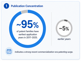
The portfolio’s 2019-2025 filing concentration shows that MicroLED patenting has remained consistently active. The patent filing pattern indicates that MicroLED innovation has moved beyond broad display-panel and emitter concepts toward implementation-level improvements directed to manufacturability, yield recovery, wafer-level integration, color conversion, optical efficiency, and pixel-level control.
Public patent examples support this trend: WO202077863A1 covers a mass-transfer apparatus, while later records address defective-pixel detection, repair structures, inspection systems, quantum-dot or photoluminescent color conversion, and thermal management.
Accordingly, MicroLED patent searches should not rely only on “MicroLED” or “micro light emitting diode,” or “Micro LED” but should also include manufacturing, integration, repair, optical, and reliability terms such as transfer head, wafer bonding, CMOS backplane, TFT driver, defect repair, redundancy, quantum dot, color conversion, microlens, light extraction, passivation, thermal management, epitaxial structure, and micro display.
6. Problems Solved by MicroLED
Hybrid-RAG addresses several limitations of conventional LLMs, keyword search, and vector-only RAG systems. The core advantage is that it combines multiple retrieval mechanisms, governance controls, and evidence-based generation to produce more accurate, traceable, and enterprise-safe answers. The table below shows the problems and their proposed solutions by Hybrid-RAG and the impact they created in the domain.
| S.No. | Problem Area | Technical Problem | Micro-LED Solution | Resulting Impact |
| 1, | Mass transfer and pitch control | MicroLED displays require the transfer of many micro-scale LED chips from a source substrate to a target display/backplane substrate. Conventional transfer approaches face limits in throughput, alignment accuracy, and pitch conversion between source and target substrates. | Uses a Micro-LED mass-transfer apparatus including die-bonding and flip-chip bonding arms, transfer heads, elastic stretchable material, an external physical-field applying device, and an operation platform to transfer MicroLEDs to target mounting positions. | Improves scalable transfer, pitch adjustment, and placement control, directly addressing one of the main bottlenecks in MicroLED panel manufacturing. |
| 2. | Thermal management, color control, and wafer integration | MicroLED chips require effective heat dissipation, insulation, wavelength/color control, and reliable bonding to a driving-circuit wafer. These issues become more critical at high pixel density. | Uses DLC thin-film layers for insulation and heat conduction, metal electrode formation, DBR filter layers, quantum-dot layers, grain isolation, N-electrode deposition, and bonding to a driving-circuit wafer. | Provides a multi-functional chip-level approach combining thermal management, color conversion, optical filtering, and wafer-level integration. |
| 3. | Full-color generation/ color conversion | Full-color MicroLED displays are difficult to manufacture using separate red, green, and blue chip transfer because different emitter materials, chip sizes, and transfer processes increase complexity and alignment burden. | Uses LED subsets covered by cured photopolymer compositions containing blue photoluminescent material and red/green nanomaterials or quantum dots for wavelength conversion. | Simplifies full-color MicroLED implementation by supporting color conversion over LED arrays, reducing reliance on separate RGB chip transfer. |
| 4. | Post-transfer repair | Defects may appear after MicroLED transfer, integration, bonding, or driver-pixel formation, creating defective pixels in the completed emissive display. | Discloses structures and repair methods for MicroLED devices and arrays to mitigate defective pixels caused by LED failure, transfer/integration defects, bonding defects, or driver-pixel defects. | Enables post-integration yield recovery, reducing panel scrap and lowering manufacturing cost for MicroLED displays. |
| 5. | Defect tolerance and redundancy | MicroLED panels are vulnerable to dead or defective sub-pixels caused by chip defects, transfer defects, or bonding failures. Even a small defect rate can severely reduce display yield. | Adds redundant MicroLED dies during manufacturing when defective dies are identified, including repaired sub-pixel assemblies with additional operative dies. | Improves manufacturing yield and commercial feasibility by allowing defective pixels/sub-pixels to be compensated rather than discarding the panel. |
| 6. | Backplane electrical testing | Defective backplane circuits are difficult to detect before final MicroLED integration. If defects are found late, material and process costs have already been incurred. | Uses a Voltage Image Optical System including an electro-optic modulator, mirrored pellicle, transparent electrode, PDLC sensor material, light source, detector, and processor to test MicroLED backplane arrays. | Enables earlier in-line inspection of backplane defects, reducing downstream yield loss and improving process control. |
| 7. | Optical extraction and ultra-dense arrays | Ultra-dense MicroLED arrays face challenges in light extraction, angular emission control, brightness efficiency, and optical crosstalk, especially for AR/VR or micro display applications. | Provides MicroLED display emitters served by corresponding microlenses, including smaller microlens geometries matched to dense emitter arrays. | Improves brightness, optical efficiency, emission directionality, and suitability for high-pixel-density MicroLED display applications. |
6.1 Summary of Technical Benefit
MicroLED solves key limitations of conventional LCD, OLED, and earlier LED display technologies. It improves brightness and efficiency through self-emissive micro-scale LEDs, improves lifetime and reliability by using inorganic semiconductor emitters, improves pixel density through wafer-level and micro-scale integration, improves manufacturability through mass-transfer, bonding, testing, and repair techniques, and improves image quality through color-conversion, microlens, and pixel-driving innovations. As a result, MicroLED is better suited for high-performance display applications where high brightness, low power consumption, long operational life, fine resolution, and scalable manufacturing are critical, including AR/VR micro displays, automotive displays, wearable devices, large-area panels, and next-generation consumer electronics.
7. Research Findings
First, MicroLED is emerging as a practical next-generation display architecture because it combines self-emissive inorganic micro-scale LEDs with advanced backplane integration, pixel-driving circuits, optical-management structures, and color-conversion techniques.
Second, patent activity has shifted from broad MicroLED emitter concepts toward manufacturing and integration improvements such as mass transfer, wafer-to-wafer bonding, CMOS/backplane integration, redundant pixel structures, repair techniques, and in-line electrical/optical testing.
Third, yield management is becoming one of the most important innovation areas, as recent patents focus on identifying defective MicroLEDs, repairing defective pixels, adding redundancy, and testing backplanes before final integration to reduce panel rejection and manufacturing cost.
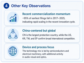
Fourth, the MicroLED portfolio further indicates that current innovation is focused on commercialization-level problems rather than basic MicroLED theory, with strong emphasis on scalable manufacturing, high-density micro displays, full-color implementation, optical efficiency, reliability, and process control.
8. Conclusion
MicroLED represents a critical evolution in next-generation display technology and display manufacturing. Conventional LCD and OLED systems solved many display-performance requirements, but they remain limited by trade-offs involving brightness, lifetime, burn-in, power efficiency, pixel density, and scalability for ultra-high-resolution applications. MicroLED addresses part of this gap by using self-emissive inorganic micro-scale LEDs, while advanced backplane integration, pixel-driving circuits, optical-management structures, and color-conversion layers improve display performance and image quality. However, the uploaded patent portfolio shows that the most commercially important innovation is no longer limited to the MicroLED emitter itself. The strongest patent activity is shifting toward scalable manufacturing and integration layers, including mass transfer, wafer-to-wafer bonding, CMOS/backplane integration, defect detection, redundant pixel structures, repair methods, backplane testing, microlens-based optical extraction, and quantum-dot color conversion. From the patent-landscape perspective, the best current direction is not a single MicroLED structure but a manufacturable MicroLED system architecture. The strongest future innovation space will likely lie in the coordination of high-yield transfer, wafer-level bonding, active-matrix driving, defect repair, optical efficiency enhancement, full-color conversion, thermal management, and in-line process verification for reliable large-scale MicroLED commercialization.